
RTL Design & Implementation of a RISC Processor and Peripheral Multiplexer -Part II

  Here is the second part of the RISC Processor Design. I have implemented this Processor as a part of my ASIC Design Lab project  "Programmable Controller/Router and Peripheral Design with peripheral I/O multiplexing".  This project focuses of peripheral multiplexing to the GPIO pins of the processor in runtime. An example case will be a Pulse Width Modulated wave switching between any I/O pins during processor execution or an UART Transmitter pin routed to a pin based on board design without the need of external multiplexers.
  The processor can access the peripherals via register write instructions. Similar to register file, the peripherals support two data reads and one data write simultaneously. Since I have used custom instructions, a custom Instruction Set Architecture (ISA) is also designed.

BLOCK DIAGRAM:


16-bit Instruction Format :


1. Register Instruction:

OPCODE [15:12]
DEST[11:8]
SRC_1 [7:4]
SRC_2 [3:0]


2. Immediate Instruction:

OPCODE [15:12]
DEST[11:8]
Immediate [7:0]

INSTRUCTION SET:


INSTRUCTION
OPCODE

INSTRUCTION
OPCODE
NOP
0000
NOT
0111
ADD
0001
MOV
1000
ADDI
0010
MVI
1001
SUB
0011
BC
1010
SUBI
0100
BS
1011
AND
0101
HLT
1111
OR
0110


REGISTER BANK:

The instructions that are supported by the CPU are mainly register instructions (R-type) and hence the register bank plays an important role in the execution of the instructions. There are a total of 16 registers available in the CPU all of which are 8 bits. The CPU registers (r0-r7) and peripheral registers share a common address space. Peripheral Address decoding is taken care by the peripherals themselves.


CPU SYNTHESIS (Synopsys Design Vision):

CPU module is synthesized and optimised in Synopsys design vision. The compiled schematic view is given below.
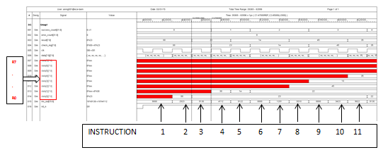

CPU VERIFICATION:


UART VERIFICATION:


TIMER VERIFICATION:


More details about individual modules will be discussed in future. 

Comments

Popular posts from this blog

Shell Scripting to Display Bar Graphs in Linux Terminal

 This week was quite hectic for me with course assignments and their merciless deadlines. One such assignment in Advanced Computer Architecture  was simulation of various benchmarks in alpha architecture in simplescalar , a well-known computer architecture simulator. I was supposed to run a total of 4 benchmarks with different configurations of cache memory, instruction issue widths, commit widths, in-order execution modes, etc and I had to plot the required performance parameters for every benchmark. A conservative estimate would be around 40 plots!  Since the simulation platform was Linux, I could breathe a sigh of relief since most things can be automated using a powerful tool called shell. Scripting made my life easier here since I can automate a bunch of simulations without having to keep an eye on each and every simulation which would take anywhere from 20 minutes to 20 hours.  The problem arose when it came to plotting the performance results. Because, each simulation

Programming STM32 ARM microcontrollers in Arch Linux

Once upon a time, not so long ago, the 8-bit microcontrollers were ruling the hobbyist embedded world. But today, the 32-bit ARM Cortex Microcontrollers are so inexpensive and power efficient that there is no good reason to ignore them. Here, let us see how to program a STM32 ARM cortex Microcontroller in Linux environment. The specific microcontroller used here is an STM32F103C8 (ARM cortex M3) programmed in Arch linux. Components Generic STM32F103 board (blue pill) STLINK-V2 (STM32 programmer) Female-Female connectors All the above components can be bought from ebay for less than $10 total. The STLINK-V2 is optional since you can use any of USB-SERIAL converters like FT232, CP2102, PL2303, CH340 and the built-in UART bootloader of STM32 chip to program. So if you already have any of the above serial converters, you don't really need STLINK to program the STM32F103 microcontroller. But STLINK helps if you plan to use in circuit debugging functionalities. Software The

JTAG - Test Access Port (TAP)Controller based Xilinx FPGA configuration using Raspberry Pi

JTAG - Joint Test Action Group is an IEEE 1149.1 standard used in many silicon devices for programming and debugging purposes. Xilinx FPGAs support this JTAG protocol for their configuration. Here I have designed a JTAG FPGA bitstream programmer using Raspberry Pi which programs the bit file into FPGA in fraction of seconds!  JTAG physical bus has four lines: TMS (Test Mode Select) TDI (Test Data In) TDO (Test Data Out) TCK (Test Clock) Components Used:  Raspberry-Pi Xilinx Spartan 3E FPGA (XC3S250E in Papilio One) Jumper wires BLOCK DIAGRAM: TAP CONTROLLER: The TAP(Test Access Port) controller is a state machine inside the FPGA which changes it's state based on TMS input. For instance, let us assume that the state machine is in " Test-Logic-Reset " state. Now if I drive the TMS pin low and toggle the TCK pin, the state machine will go to " Run-Test/ Idle " state. This is how we move to different states.  Note